Eagle: Difference between revisions
adding svg files |
|||
| (30 intermediate revisions by 4 users not shown) | |||
| Line 1: | Line 1: | ||
See version in Icelandic [[ | See version in Icelandic [[Eagle kennsluefni]] | ||
[[Image:eagle_layout.png|right|x400px|eagle_layout.png]] | |||
[[:File:eagle_layout_svg.svg]] | |||
== Download and install Eagle == | |||
*[http://www.cadsoftusa.com/download.htm Download Eagle] | *[http://www.cadsoftusa.com/download.htm Download Eagle] | ||
==Designing circuits with Eagle== | === Linux 64-bit === | ||
Eagle requires a 32-bit environment which may or may not be installed in linux yet.<br /> | |||
I have taken the step to istall the following libraries prior to running the eagle.run file from [http://blog.raek.se/2012/01/06/running-cadsoft-eagle-version-6-in-ubuntu-gnulinux/ here] | |||
<pre>sudo apt-get install ia32-libs lib32z1 lib32z1-de</pre> | |||
After this eagle installed without a problem. | |||
=== Linux alt-click / alt-drag moving the window problem === | |||
The newer Linux window managers tend to use the alt-click or alt-drag combinations to move or re-size windows. This prevents us from using that same key in both Blender and Eagle. | |||
tip about using alt-grid on ubuntu: | |||
*http://www.thomasso.com/2014/05/03/changing-keyboard-short-cuts-in-ubuntu-14-04-to-work-with-blender-2-70/#sthash.EoyaD0aa.dpbs<br /> | |||
but also look into changing this behavior from the regular window manager. (as it is apparently not a keyboard shortcut...) | |||
For Linux Mint 17, the following trick was used: | |||
*http://forums.linuxmint.com/viewtopic.php?f=90&t=108974#p660925 | |||
== Designing circuits with Eagle == | |||
[[File:eagle_tool_commands.png|right|eagle_tool_commands.png]] | |||
Open Eagle | Open Eagle | ||
*Select New Project | |||
*Select New Project | |||
*Select New Schematic | *Select New Schematic | ||
Open library | Open library | ||
* Open | turn off all libraries, right click use none: | ||
*Download from the internet a library or select on in the computer the library that we will be using (e.g. | scroll down to supply | ||
enable | |||
*fab.lbr | |||
*supply1.lbr | |||
*rcl.lbr | |||
*led.lbr | |||
*v-reg.lbr | |||
*Open library, click '''Use''' | |||
*Download from the internet a library or select on in the computer the library that we will be using (e.g. | |||
*fab.lbr[http://fabacademy.org/archives/2014/tutorials/electronics/fab.lbr] | |||
*or the one from Sparkfun.lbr ([http://www.opencircuits.com/SFE_Footprint_Library_Eagle] version 2011 ( [https://github.com/sparkfun/SparkFun-Eagle-Library/blob/master/SparkFun.lbr?raw=true right click on this link, save link as]) | |||
*Select'''Add''', then you can open the library | |||
**(if you don't find your thing you could also click on "Use") | |||
<br> [http://www.cadsoftusa.com/Tour/tour00.htm Tour for the Eagle on CadSoft site] | |||
<br> | |||
[[:File:tool_comads_eagle_svg.svg]] | |||
==Starting new projects== | |||
*File -> New Project | |||
*File -> New Schematic | |||
*File -> Save As (filename.sch) | |||
*Select the things you want to use and click '''Add''' to get the components. | |||
*You can select different view by clicking on '''Board''' | |||
*You can select object by right clicking them and selecting packning | |||
*Connect objects by clicking '''Wire''' and make wire between objects. | |||
*It can be good to make connections and get a sign for Ground and put where it should be GND. | |||
*View '''Grid''' select the size of the grid, | ===Board view=== | ||
* ''' Move''' to move object or line. | *View '''Grid''' select the size of the grid, alternative grid could be around (0,025 inches) | ||
*'''Delete''' to remove object or line and so on. | *'''Move''' to move object or line. | ||
*'''Junction''' Connection point . | *'''Delete''' to remove object or line and so on. | ||
*'''Junction''' Connection point . | |||
*'''Ratsnest''' Calculates calculate the airwires so that they show the shortest possible connections. | |||
**You can right click objects and select '''value''' to set values e.g. for capacitors or resistors | **You can right click objects and select '''value''' to set values e.g. for capacitors or resistors | ||
**Right click on object and select '''properties''' to rename. | **Right click on object and select '''properties''' to rename. | ||
**You can check out if you have connected the object by moving them. | **You can check out if you have connected the object by moving them. | ||
*'''ERC''' | *'''ERC''' Electrical rule check, search for errors. | ||
===Arrange objects === | |||
====Arrange objects==== | |||
A tip for arranging objects | |||
*Start with data signals, and do your power signals (GND and VCC the last). | |||
Add | Add | ||
*'''Frame''' to make frame around the design. | |||
Check the design rules. | |||
*Tools ->DRC -> Load-> Check | |||
*'''Frame''' to make frame around the design. | |||
*Arrange objects | *Arrange objects | ||
*click '''Auto''' | *click '''Auto''' | ||
**Select Bottom N/A | **Select Bottom N/A | ||
If it is not as good as you wanted you can select lines, by right clicking them and select '''rip off''' | If it is not as good as you wanted you can select lines, by right clicking them and select '''rip off''' | ||
<br> | |||
View-> Layer settings -> | |||
*All ->Ok ( to check out if everything is within the board, also the layers that are not visible. | |||
*None -> | |||
and the turn on the layers you want to have. | |||
*File -> Export image | |||
**resolution: 1200 dpi | |||
**Area: Full | |||
*Monochrome: check. | |||
== Info about Circuits == | |||
*TX transmit | |||
*DTR data terminal ready | |||
*Rx Recieve | |||
*Miso -master in slave out | |||
*Mosi master out slave in | |||
*sck system clock | |||
*MOSI (3) GND (2) MISO (1) | | |||
*-RESET (4) SCK (5) | |||
== | == Project 1 == | ||
* | *First project could be to make schematic of this board and to add something to it, add (at least) a button and LED (with current-limiting resistor) to the serial echo hello-world board, check the design rules, and make it | ||
* | **[http://fab.cba.mit.edu/about/fab/hello/ftdi/hello.ftdi.44.png See the layout for hello.ftdi.44] | ||
*Download libraries | |||
**fab.lbr[http://fabacademy.org/archives/2014/tutorials/electronics/fab.lbr] | |||
*Download libraries | |||
** | |||
**[http://www.mikrocontroller.net/attachment/68243/atmel-new.lbr atmel-new.lbr, Attiny 44 library] | **[http://www.mikrocontroller.net/attachment/68243/atmel-new.lbr atmel-new.lbr, Attiny 44 library] | ||
==Links== | === Materials used === | ||
*[http://www.cadsoftusa.com/Tour/tour00.htm Eagle Tour] | |||
*[http://perso.numericable.fr/pboucheny/eagle3d/e_genpov.htm HOW TO GENERATE POV-RAY FILES WITH EAGLE] | *IC1 = ATtiny44_SOIC('IC1\nt44') -> see in fab.lbr | ||
*[http://www.matwei.de/doku.php?id=en:eagle3d:eagle3d Eagle 3D] | *R1 = R_1206('R1\n10k') -> See in fab.lbr | ||
*C1 = C_1206('C1\n1uF') -> fab.lbr | |||
*XTAL = Crystal 20 MHz -> search for crystal in fab.lbr | |||
*FTDI connector (6 pin) ->search for ftdi in fab.lbr | |||
*Header (2*3 pin) -> search for isp in fab.lbr | |||
== Links == | |||
*[http://www.cadsoftusa.com/Tour/tour00.htm Eagle Tour] | |||
*[http://www.cadsoft.de/wp-content/uploads/tutorial-7.1_en.pdf Eagle Tutorial 7.1] | |||
*[http://perso.numericable.fr/pboucheny/eagle3d/e_genpov.htm HOW TO GENERATE POV-RAY FILES WITH EAGLE] | |||
*[http://www.matwei.de/doku.php?id=en:eagle3d:eagle3d Eagle 3D] | |||
*[http://academy.cba.mit.edu/content/tutorials/eagle/eagle_resources.html http://academy.cba.mit.edu/content/tutorials/eagle/eagle_resources.html] | |||
[http://fab.cba.mit.edu/classes/MIT/863.10/people/dimitris.papanikolaou/Assignment_6.html http://fab.cba.mit.edu/classes/MIT/863.10/people/dimitris.papanikolaou/Assignment_6.html] | |||
== Videos == | |||
*[http://www.youtube.com/watch?v=qG0O9LKH-_E Cadsoft EagleCad Tutorial on Youtube] | |||
[[Category:Tutorials]] [[Category:Software]] | |||
Latest revision as of 18:25, 26 February 2016
See version in Icelandic Eagle kennsluefni

Download and install Eagle
Linux 64-bit
Eagle requires a 32-bit environment which may or may not be installed in linux yet.
I have taken the step to istall the following libraries prior to running the eagle.run file from here
sudo apt-get install ia32-libs lib32z1 lib32z1-de
After this eagle installed without a problem.
Linux alt-click / alt-drag moving the window problem
The newer Linux window managers tend to use the alt-click or alt-drag combinations to move or re-size windows. This prevents us from using that same key in both Blender and Eagle.
tip about using alt-grid on ubuntu:
but also look into changing this behavior from the regular window manager. (as it is apparently not a keyboard shortcut...)
For Linux Mint 17, the following trick was used:
Designing circuits with Eagle

Open Eagle
- Select New Project
- Select New Schematic
Open library turn off all libraries, right click use none: scroll down to supply enable
- fab.lbr
- supply1.lbr
- rcl.lbr
- led.lbr
- v-reg.lbr
- Open library, click Use
- Download from the internet a library or select on in the computer the library that we will be using (e.g.
- fab.lbr[1]
- or the one from Sparkfun.lbr ([2] version 2011 ( right click on this link, save link as)
- SelectAdd, then you can open the library
- (if you don't find your thing you could also click on "Use")
Tour for the Eagle on CadSoft site
File:tool_comads_eagle_svg.svg
Starting new projects
- File -> New Project
- File -> New Schematic
- File -> Save As (filename.sch)
- Select the things you want to use and click Add to get the components.
- You can select different view by clicking on Board
- You can select object by right clicking them and selecting packning
- Connect objects by clicking Wire and make wire between objects.
- It can be good to make connections and get a sign for Ground and put where it should be GND.
Board view
- View Grid select the size of the grid, alternative grid could be around (0,025 inches)
- Move to move object or line.
- Delete to remove object or line and so on.
- Junction Connection point .
- Ratsnest Calculates calculate the airwires so that they show the shortest possible connections.
- You can right click objects and select value to set values e.g. for capacitors or resistors
- Right click on object and select properties to rename.
- You can check out if you have connected the object by moving them.
- ERC Electrical rule check, search for errors.
Arrange objects
A tip for arranging objects
- Start with data signals, and do your power signals (GND and VCC the last).
Add
Check the design rules.
- Tools ->DRC -> Load-> Check
- Frame to make frame around the design.
- Arrange objects
- click Auto
- Select Bottom N/A
If it is not as good as you wanted you can select lines, by right clicking them and select rip off
View-> Layer settings ->
- All ->Ok ( to check out if everything is within the board, also the layers that are not visible.
- None ->
and the turn on the layers you want to have.
- File -> Export image
- resolution: 1200 dpi
- Area: Full
- Monochrome: check.
Info about Circuits
- TX transmit
- DTR data terminal ready
- Rx Recieve
- Miso -master in slave out
- Mosi master out slave in
- sck system clock
- MOSI (3) GND (2) MISO (1) |
- -RESET (4) SCK (5)
Project 1
- First project could be to make schematic of this board and to add something to it, add (at least) a button and LED (with current-limiting resistor) to the serial echo hello-world board, check the design rules, and make it
- Download libraries
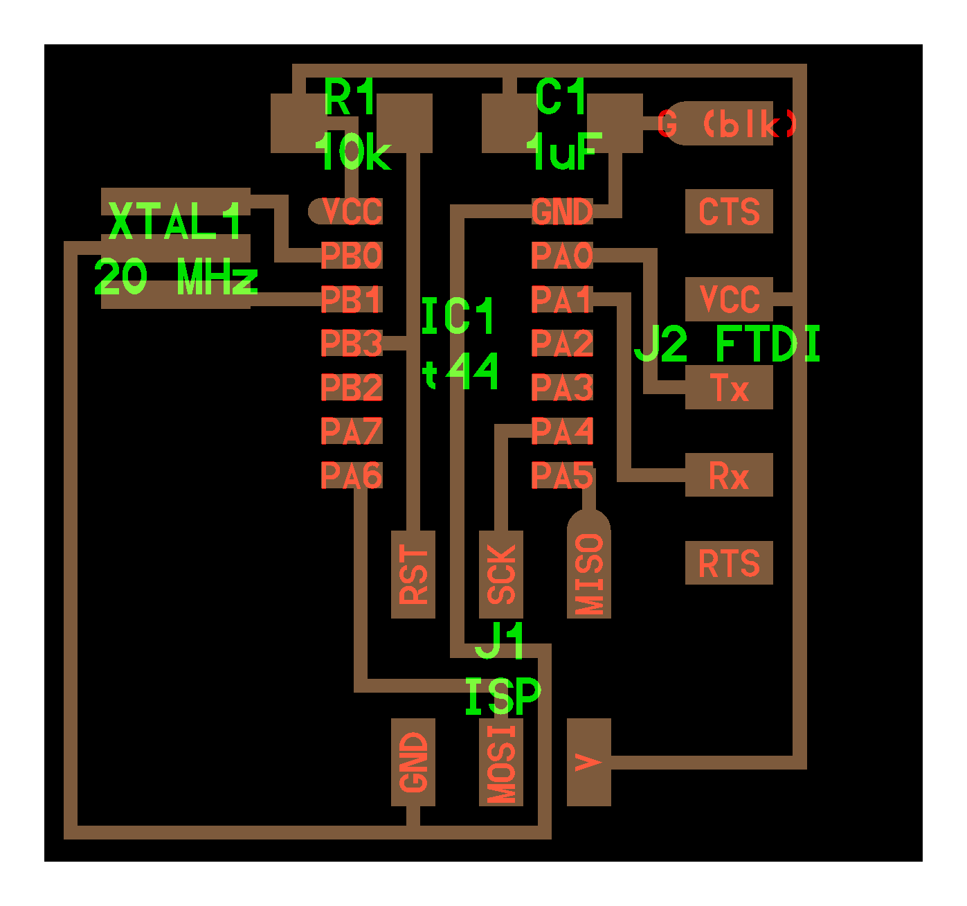
Materials used
- IC1 = ATtiny44_SOIC('IC1\nt44') -> see in fab.lbr
- R1 = R_1206('R1\n10k') -> See in fab.lbr
- C1 = C_1206('C1\n1uF') -> fab.lbr
- XTAL = Crystal 20 MHz -> search for crystal in fab.lbr
- FTDI connector (6 pin) ->search for ftdi in fab.lbr
- Header (2*3 pin) -> search for isp in fab.lbr
Links
- Eagle Tour
- Eagle Tutorial 7.1
- HOW TO GENERATE POV-RAY FILES WITH EAGLE
- Eagle 3D
- http://academy.cba.mit.edu/content/tutorials/eagle/eagle_resources.html
http://fab.cba.mit.edu/classes/MIT/863.10/people/dimitris.papanikolaou/Assignment_6.html